Fan Out Embedded Die Interposer
FOED is an advanced wafer level package (WLP) technology that offers significant improvements on performance over traditional packaging methods.
Product Solution with Fan Out Embedded Die Interposer (FOED) Packaging
At TF-AMD Penang, we offer Advanced Packaging Platform of FOED. This product solution covers 3 major technologies:
 uBumping, including uStud
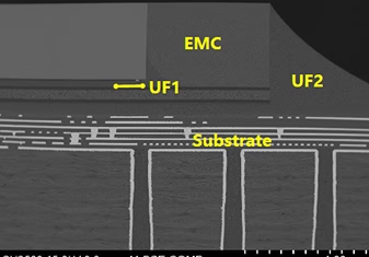
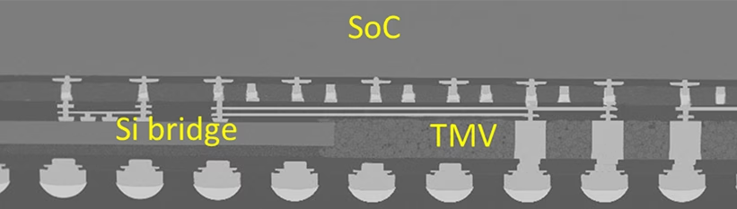
2D+ FO with Embedded Die Interposer (FOED)
Fan Out Package on Substrate (FOPoS)
This solution allows for design flexibility, high-performance, miniaturized, and cost-effective packaging solution for today’s most demanding applications, from 5G+ mobile phones to AI assistance and beyond.
Key Benefits Of FOED:
Higher I/O density: With sub-micron interconnection at embedded die and sub-10um interconnection at FO interposer, it provides scalable high density interconnection between chips and chiplets.
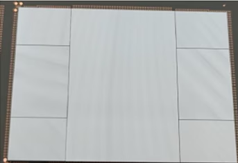
Design Architecture Flexibility: The 2D+ structure provides flexible floor plan for logic, I/O and memory chips or module in FOED package.
Improved heat dissipation: The structure with exposed main Si die backside and optional backside metallization, together with dense Cu post at FO interposer, provides better thermal management capability and flexibility.
Cost Efficiency: Lower overall packaging costs compared to 2.5D TSV Interposer package. Enabler for chiplet technology.
Smaller form factor: With 2D+ scalable vertical construction, it is ideal for space-constrained applications like mobile devices, wearables, and IoT.
Advanced Packaging Platform Of FOED Services Offers:
End-to-end one stop solution: uBump (micro-bumping), FOEB, oS (on-substrate assembly) , CP and Test solution at one manufacturing plant, TF-AMD (Penang) at Batu Kawan.
Design and Simulation: Comprehensive design and simulation services to ensure optimal package performance, especially reliability projection.
Prototype and Pilot Production: Fast-track your product from concept to small-volume production with one-time NPI qualification pass.
Full-Scale Manufacturing: Scalable solutions for mass production with guaranteed quality and cycle time.
Testing and Reliability Assurance: Rigorous testing to meet industry standards for reliability and performance.
FOED Features
| Wafer Size | 300mm |
| Module Size | 12x12mm to 52x68mm |
| Die Quantity per Module | 5 to >=28 |
| Embedded Die Quantity in Interposer | 3 to 25 |
| RDL layer | 2P2M to 4P4M |
| RDL L/S (um) | 2/2um to 10/10um |
Reliability Test Standards
The test criterion is JEDEC Precondition MSL-4:J-STD-20/JESD22-A103
| Preconditioning | High Temp Storage Test |
| Temp Cycle Test | -65 ~ 150°C, 800cycles, JEDEC22-A104 |
| uHAST | 130°C / 85% RH, 192hr, JEDEC22-A118 |
| High Temp Storage Test | 150°C, 1500hrs, JEDEC 22- A103 |
Example: